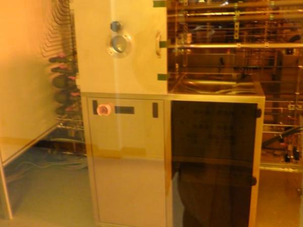
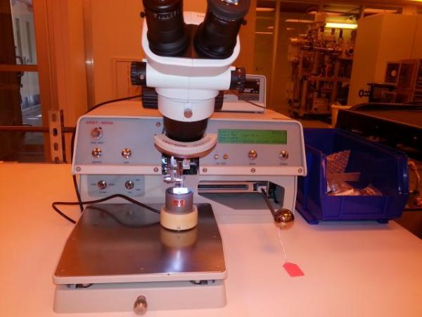
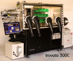
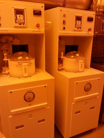
The UNT Nanofabrication Cleanroom has a wide selection of processing tools, including
dual e-Beam, thermal evaporation and sputtering systems for thin film development,
and two RIE systems for metal and dielectric material etching of MEMS structures.
Sub-micron features are defined with a JEOL JSM-7001F SEM/EBL system with 3nm beam
resolution and a Heidelberg DWL66fs maskless laser writer for photomask pattern writing.
Four wet benches, HMDS 15 oven and spin coater hood with tabletop spin coater (Laurell
WS-650Mz) are used for lithography process. For characterization analysis, the cleanroom
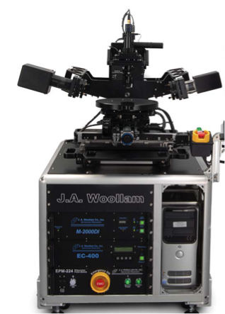
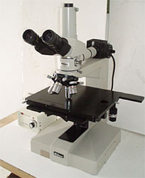
is equipped with a J.A. Woolam M-2000V Ellipsometer and Nikon 66 microscope.
For current availible tools, please check Tool Status. For tool scheduling, please check UNT FOM.
Equipment

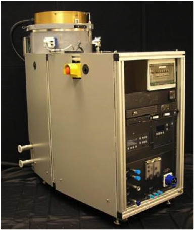
The MPS-RIE is great for day-to-day use at the push of a button.
- Best built R&D or low volume production tool available
- SiO2, SiNx, TiW, GaAs, resist, ILD and polyimide, micromachining (MEMS), photonics,
HTSC's, and for failure analysis
- Accepts any size substrate from 1" to 6" wafers, flat panels, or custom packages
- Easy to use and simple to service
- Safe, rugged design means high reliability with remarkable uptime
- Simple 5 piece chamber construction is versatile and easy to upgrade
- Multi-use process kit with virtually no process memory effect

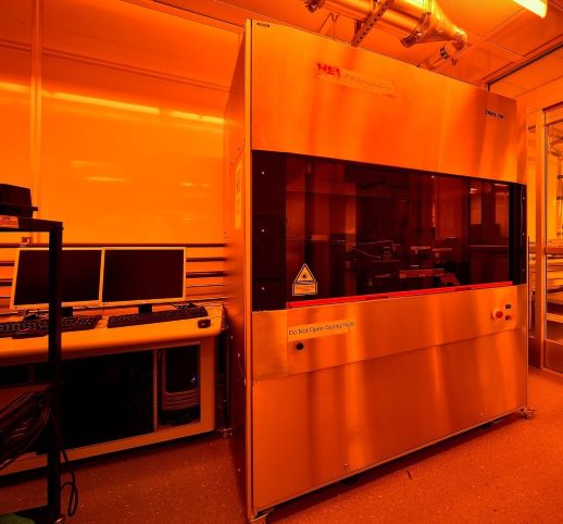
The DWL 66 is a high precision, direct write laser lithography system for:
- Maskless lithography
- Photomask making
- Direct writing applications
- Gray-scale exposures
- Any flat material coated with a photosensitive layer
Main features include:
- Minimum feature size: 0.6 microns
- Substrate size: Up to 200 x 200 mm (8 x 8 inches)
- Over 1.0M dpi using a 20-nanometer writeable address grid

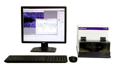
- Vertical range 0-1000 microns
- Low force measurement at 0.05 to 15 mg
- Step height repeatability of 0.1 nm of 10 nm step
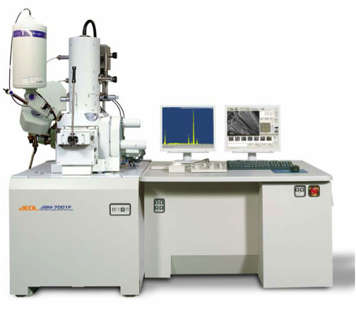
The JSM-7001F analytical thermal field emission SEM is the ideal platform for demanding
analytical applications as well as those requiring high resolution and ease-of-use.
The JSM-7001F has a large, 5-axis, fully eccentric, motorized, automated specimen
stage, a one-action specimen exchange airlock, small probe diameter even at large
probe current and low voltage, and expandability with ideal geometry for EDS, WDS,
EBSP, and CL. The specimen chamber handles specimens up to 200mm in diameter.

JSM-7001F Key Product Features
Resolution
(secondary electron image)
1.2 nm (at 30 kV)
3.0 nm (at 1.0 kV)
3.0 nm (at 15 kV 10mm WD, 5nA)
Accelerating Voltage
0.5 to 2.9 kV (10V steps)
3.0 to 30 kV (100V steps)
Magnification
x10 to 1,000,000x (printed as a 120mm x 90mm micrograph)
Imaging Modes
SEI (secondary electron image)
BEI to E/T Detector
BEI - Option (backscattered electron
image TOPO and COMPO
Resolution
(secondary electron image)
- 1.2 nm (at 30 kV)
- 3.0 nm (at 1.0 kV)
- 3.0 nm (at 15 kV 10mm WD, 5nA)
Accelerating Voltage
- 0.5 to 2.9 kV (10V steps)
- 3.0 to 30 kV (100V steps)
Magnification
- x10 to 1,000,000x (printed as a 120mm x 90mm micrograph)
Imaging Modes
- SEI (secondary electron image)
- BEI to E/T Detector
- BEI - Option (backscattered electron image TOPO and COMPO)
The M-2000 line of spectroscopic ellipsometers is engineered to meet the diverse demands
of thin film characterization. An advanced optical design, wide spectral range, and
fast data acquisition make it an extremely powerful and versatile tool.

Wavelength Range:
- M2000V 370-1000nm, 390 wavelengths
Angle Range:
- Fixed Angle 65°
- Manual Angle 45° - 90°
- Horz. Auto Angle 45° - 90°
- Vert. Auto Angle 20° - 90°
- MASE 45°, 60°, 75°
- Focusing 65°
System Overview:
- Patented rotating compensator ellipsometry, simultaneous CCD detection of all wavelengths,
flexible system integration
- Data Acquisition Rate: Data collected 20 times per second.
- For optimal signal-to-noise, typical measurement times for full spectrum is between
0.5 and 5 seconds.
5X, 20X, 40X,100X objective, 6” x 6” right-hand X-Y Stage, Rotating Polarizer 360
degrees


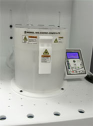
The Laurell WS-650 Spin Coater is compact and packed with advanced features. This
650-series coater system will accommodate up to ø150mm wafers and 5" × 5" (127mm ×
127mm) substrates, and features a maximum rotational speed of 12,000 RPM (based on
a ø100mm silicon wafer).
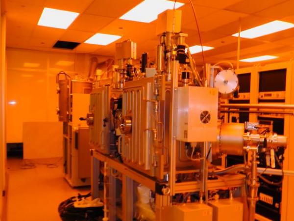
Oerlikon Ion Assist Ebeam and Sputtering system:
Substrate heater: up 1000 degree C.


Nano-Master, Inc. NEE-4000 Electron Beam Evaporation Systems come in a dual chamber
configuration consisting of the main chamber where platen is located and a secondary
chamber for housing the e-beam source. This configuration with a gate valve between
two chambers may be used as a load lock to keep the e-beam source pockets in vacuum
while substrate is loaded and unloaded from the main chamber substrate holder or platen.
On other applications where automatic loading and unloading of wafers is needed, it
can be achieved through a third load lock chamber that may be attached to the left
face of the cube. Co-evaporation capability with multiple e-beam sources and ability
to program compositions or compositional gradients through PC control can be provided.


- Fully Automated Vacuum and Process Control
- 4 Material Co-Deposition
- Proprietary Ultra-High Resolution QCM Monitoring
- PC Based Multi-Layer Thin-Film Process Control
- 12 Evaporative Sources
- Multiple Substrate, In-Process Mask Changing
- Cryogenic Pumping - 12 Minutes to Process Pressure
- Integrated Glove Box System <1PPM -H2O, O2
- Vacuum Antechamber for Glovebox
- Compact Footprint - 114" Wide x 36" Deep x 76" High
- Optional Integrated Spin Coater, UV Ozone, Encapsulation

Laurell WS-1000MH -CP7-D Mini chemcial processing stations:
for photomask etching, development and Photolithography liftoff
Status
User are responsible for bringing necessary material for processing, e.g. photoresist,
development etc. Any material brought into cleanroom is subject to cleanroom manager
for review.
Currently availble tools:
- Heidelberg DWL-66s laser writer
- JEOL JSM-7001F SEM and EBL XPG2 pattern generator
- Laurell WS-650 Mz spin coater
- Reactive Ion Etcher (dielectric material)
- HP61 hot plate
- Nikon optphot 66
- KLA-Tencor D300 Profiler
- UV Ozone cleaner
- West Bond Wire Bonder
- Nanomaster Dual Ebeam Evaporator
- J.A. Woolam Co., Inc. M-2000V Automated Angle Ellipsometer
- Oerlikon Sputtering & Ebeam system
- Trovato organic deposition
- Chemical processing station for photomask developing and liftoff
